How to increase the current source/sink capacity of a digital PWM signal

In summary, the circuit proposed by Mike will work, is single chip, and has a smaller footprint. There may be other components that are needed, depending on the load that is being driven, but the gate driver should be sufficient.
  • #1
Mark Merlo
2
0
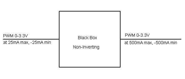
I would like to increase the maximum current that a PWM signal from a microcontroller can source/sink from +-25mA to +-500mA.
attachment.php?attachmentid=26759&stc=1&d=1277851528.png


The output should have the same peak-to-peak voltage (0 to 3.3V) and should not be inverted (i.e. follows the input). The PWM frequency is ~30kHz. I have looked into using an active push-pull output but the only configuration I can find is inverting. Since the output needs to follow the input, I need to invert the input. I found this chip with complementary mosfets that looks like it would work for the output stage: http://search.digikey.com/scripts/DkSearch/dksus.dll?Detail&name=DMG1016V-7DICT-ND and this chip for the input BJT inverting stage: http://search.digikey.com/scripts/DkSearch/dksus.dll?Detail&name=MMDT2227MDICT-ND
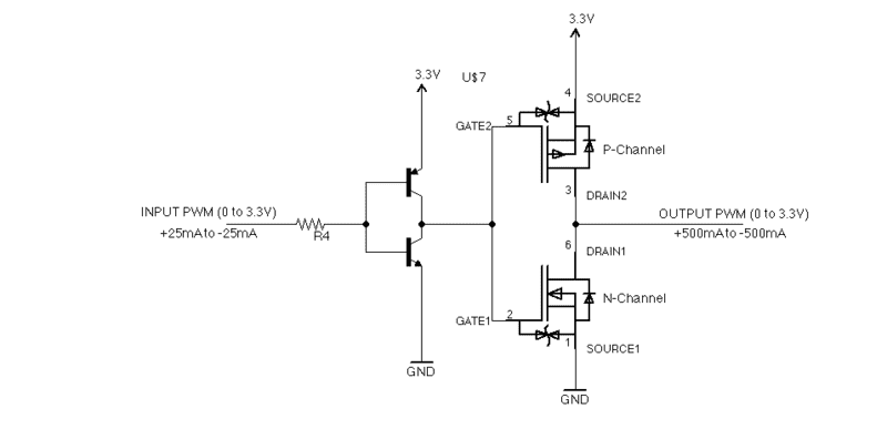
Here is my proposed circuit:
attachment.php?attachmentid=26760&stc=1&d=1277851528.png


The output stage mosfets have fairly small total gate charge of ~700pC each, so I think I could drive them directly with my microcontroller if I could find a non-inverting configuration.

So my questions are:
1. Will this circuit work?
2. Is there a single chip solution?
3. Is there a better circuit that would fit my needs (less components, cheaper, smaller footprint)?
4. Is there anything that I am missing? Diodes, resistors, etc?

Also, I do not have a specific load that I am driving, this is more of a generic output that can drive different load types. I would like to make this +-500mA source/sink PWM as similar to a uC output, but with larger current sourcing and sinking capacity.

Thanks for the help.
 

Attachments

  • blackbox.png
    blackbox.png
    881 bytes · Views: 1,557
  • proposed circuit.png
    proposed circuit.png
    6.5 KB · Views: 3,504
Last edited by a moderator:
Engineering news on Phys.org
  • #2
The way you have your BJT's installed will get you high currents through the top emitter, on through it's base, into the bottom transistor's base and through it's emitter. That's about 1.2 volts drop and a very heavy current draw.

It's too bad your not going for something with a bit less current or a bit more voltage.
For less current, I'd just parallel up the outputs of some CMOS line drivers. Tie the outputs together through some 22 ohm resistors and viola' you can have 8 gates driving in parallel capable of a good 150ma. Just be sure the gates are driven by a, clean edge, or some may come on before the others and they'd fight each other at each transistion (that's what the resistors are for anyway)

As for higher voltage, gate drivers can definitely deliver a punch, but finding one that operates with a 3.3 volt supply might be a challenge.

As for this thing with two MOSFETs, you have to be careful that they don't both turn on during switching, or you'll have shoot through current through the MOSFETs. This causes RF noise, heat, general nastiness. You can probably rig a gate driver for each of the MOSFETs with a resistor, capacitor, diode combination, so that the FETs are turned on with a tiny delay (due to the charging of the RC) and turned off suddenly (discharging the C through the diode). As for driving the MOSFETs, if you use small ones, you can generally drive them from a CMOS gate.

Best Luck,

- Mike
 
  • #3
Thanks Mike, everything you say makes perfect sense. I am really glad that you explained the issue with my BJT configuration. I actually saw this configuration in Horowitz and Hill under the "Bad Circuit" section. The circuit was labeled as a follower, but it looked like an inverting circuit to me at the time, so I figured that it was a bad circuit because it did not follow the input. Now I see the issue, because of the forward voltage drops, both BJTs will always be biased and on. No doubt these transistors will burn up quickly. I guess this push-pull configuration works for mosfets because they are voltage controlled and do not have a forward voltage drop.

You are right, my requirements are at odds with each other. I have opted to increase my output voltage to 0 to 5V. With this change, it looks like Microchip's MCP1402 gate driver should do the trick. I can drive it with my 3.3V signal and it can delivery +-500ma output at 0-5V. The one thing that I am unsure of is if I need to put two clamping diodes (one to 5V and one to gnd) on the output of the gate driver since I might be driving an inductive load. The output is never in a high impedance state so there should not be any inductive voltage kick and the chip has up to 500mA reverse current latch-up rating. So, do I need to put clamping diodes on the output? Is there any other additional circuitry/components that are need with the gate driver? As it stands now, I only have the gate driver chip with a couple of bypass caps.

Thanks again for the help.
 

Related to How to increase the current source/sink capacity of a digital PWM signal

1. How does increasing the voltage affect the current source/sink capacity of a digital PWM signal?

Increasing the voltage can increase the current source/sink capacity of a digital PWM signal. This is because the higher the voltage, the more energy is available to drive the signal and increase its capacity.

2. Can the current source/sink capacity of a digital PWM signal be increased without changing the voltage?

Yes, the current source/sink capacity can also be increased by using a higher power supply or by using amplifiers or buffers to boost the signal.

3. Are there any limitations to increasing the current source/sink capacity of a digital PWM signal?

Yes, there are limitations such as the maximum voltage and current that the components can handle, as well as the design and layout of the circuit. It is important to carefully consider these limitations when attempting to increase the capacity of a digital PWM signal.

4. How can I determine the current source/sink capacity of a digital PWM signal?

The current source/sink capacity of a digital PWM signal can be determined by calculating the maximum voltage and current that the components in the circuit can handle, as well as considering the design and layout of the circuit.

5. Are there any other methods besides increasing the voltage and using amplifiers to increase the current source/sink capacity of a digital PWM signal?

Yes, other methods include using higher grade components with higher maximum voltage and current ratings, optimizing the layout and design of the circuit, and implementing efficient and advanced techniques such as pulse skipping or pulse frequency modulation.

Similar threads

Replies
25
Views
5K
Replies
47
Views
3K
Replies
1
Views
3K
  • Electrical Engineering
Replies
16
Views
2K
  • Electrical Engineering
Replies
20
Views
6K
  • Electrical Engineering
Replies
3
Views
2K
  • Electrical Engineering
Replies
24
Views
4K
  • Electrical Engineering
Replies
12
Views
2K
Replies
2
Views
4K
  • Electrical Engineering
Replies
1
Views
5K
Back
Top